My Semiconductor Cleanroom Experience at ASU NanoFab
- Nirav Shah
- Mar 3, 2025
- 3 min read

Updated: Mar 3, 2025

I undertook a course with Prof. Trevor Thornton called Fundamentals of CMOS and MEMS which exposed me to ASU's NanoFab and various process steps. Albeit we weren't allowed to carry out the procedures, we did generate data once a process step was completed (oxide growth, RI etching, deposition) and then characterized the data to analyze the equipment and understand semiconductor properties.
Scanning Electron Microscopy
We kicked things off by getting acquainted with a powerful analytical tool - the Scanning Electron Microscope (SEM). Using a Phenom Pro SEM, we examined a 1 micron grating test sample at 12,500x magnification.
The SEM works by focusing a beam of electrons onto a sample surface to generate high-resolution images. This allows us to visualize features far smaller than optical microscopes can resolve.
Some key takeaways:
• We achieved 98.98% measurement accuracy on the grating
• Proper sample positioning is crucial for optimal focus
• SEMs enable detailed surface analysis at the micro and nanoscale


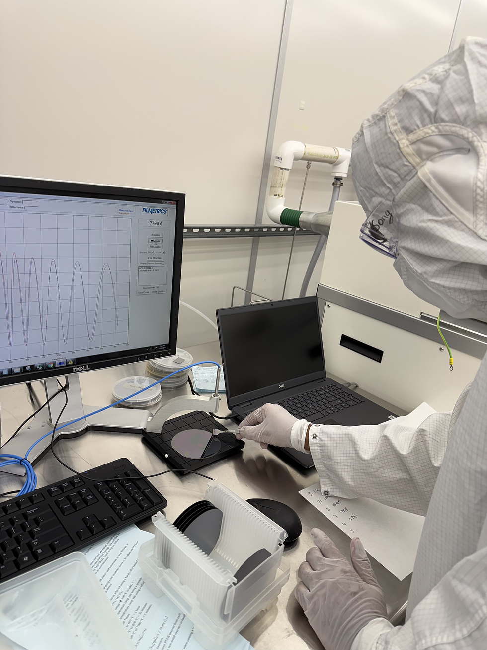
Thermal Oxidation - Part 1
Next, we dove into thermal oxidation - a fundamental process for creating insulating layers in semiconductor devices. We oxidized silicon wafers in a furnace and measured the resulting oxide thickness.
The process involved:
1. Thorough wafer cleaning (RCA and piranha cleans)
2. Controlled oxidation in a Tystar furnace
3. Precise thickness measurements using a Filmetrics reflectometer
By analyzing our data, we were able to extract key parameters of the Deal-Grove oxidation model and were able to predict oxide growth rates for different conditions.
Thermal Oxidation - Part 2
Building on our experimental work, we used Silvaco simulation software to model the thermal oxidation process. This allowed us to compare simulated results with our actual measurements.
Key findings:
• Simulated oxide thickness was consistently lower than measured values
• At 1050°C, we saw good agreement between simulation and experiment
• Lowering the temperature to 900°C significantly slowed oxide growth

The simulation exercise demonstrated how computational tools can complement and enhance experimental work in semiconductor processing.
Photolithography
Photolithography is a crucial process in semiconductor fabrication, allowing us to transfer intricate patterns onto wafers. Our lab experience focused on creating precise structures using this technique.
Key steps we performed:
1. Wafer cleaning and dehydration baking
2. Photoresist application via spin coating
3. Soft baking to remove solvents
4. UV exposure through a mask
5. Development to reveal the pattern
We used both positive and negative resists, observing how each responds differently to UV light. The positive resist became more soluble in exposed areas, while the negative resist polymerized and became less soluble.
Challenges we encountered:
• Achieving uniform photoresist coating
• Aligning the mask precisely
• Controlling exposure time for optimal pattern transfer
Through this hands-on experience, we gained a deep appreciation for the precision required in modern semiconductor manufacturing.
Reactive Ion Etching
Following photolithography, we delved into Reactive Ion Etching (RIE), a technique used to selectively remove material from wafer surfaces.
Our RIE process involved:
1. Loading patterned wafers into the RIE chamber
2. Introducing specific gas mixtures (CF4 and O2)
3. Generating plasma to create reactive species
4. Controlling parameters like power, pressure, and gas flow
We etched silicon dioxide layers, measuring etch rates and examining the resulting structures. Key observations included:
• Increased RF power led to faster etch rates
• The CF4:O2 ratio significantly affected etch selectivity
• Proper endpoint detection was crucial to avoid over-etching
This module highlighted the importance of precise process control in achieving desired etch profiles and maintaining feature integrity.
MOSFET Characterization
In our final lab, we characterized MOSFET (Metal-Oxide-Semiconductor Field-Effect Transistor) devices, the building blocks of modern electronics.
We performed several key measurements:
1. ID-VG characteristics to determine threshold voltage
2. ID-VD curves to observe different operating regions
3. Subthreshold swing analysis
4. Channel length modulation effects
Using a four-probe station and parameter analyzer, we extracted important device parameters:
• Threshold voltage (VT)
• Transconductance (gm)
• Subthreshold slope
• Channel length modulation parameter (λ)
We compared our experimental results with theoretical predictions, gaining insights into real-world device behavior and the impact of fabrication variations.
This series of labs provided a comprehensive, hands-on introduction to key semiconductor fabrication processes. From imaging at the nanoscale with SEM to creating and characterizing actual transistors, I gained some cool practical experience!

Comments